Building a Quantum Computer in Reverse
By Nick Farina
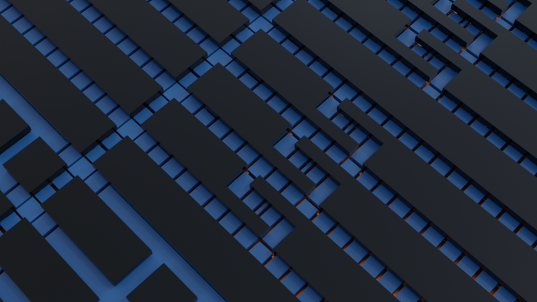
Scaling has long been recognized as a major hurdle for quantum processors, along with a need for advances in quantum error correction and the control of quantum gates.
However, while rapid progress has been made in the latter two, far less progress has been made in the development of a CMOS-based scalable system, where the devices and qubits are sufficiently identical that the number of external control signals increases slowly with the number of qubits.
Therefore the development, taping-out, and functionality of a CMOS-based scaling architecture has taken on new significance, as scaling has become the most critical remaining task for building a commercially viable quantum computer.
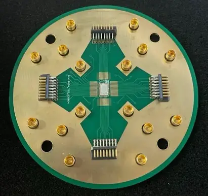
At EeroQ, we have made a key advance towards this goal, achieving tape-out and demonstrating functionality of a 2,432 future qubit system, which we’re calling Wonder Lake. Our Wonder Lake chips were fabricated at a major US semiconductor foundry and use only ~30 control lines, solving some of the major scaling problems faced by certain other qubit platforms.
The architecture of a quantum processor requires multiple layers, all of which work in concert. In this post, we will go into some of the details about the layers of our chip. This chip will form the infrastructure needed for future devices that can hold single electrons, which we are working to develop as a leading qubit platform.
With our announcement today, we offer a credible path to allow our systems, which are based on the isolated electron spins trapped above the surface of liquid helium (eHe), to scale from single qubits to 10,000 and beyond… by starting from scale, and building a quantum computer in reverse.
Backstory: Using isolated electron spins on helium as a qubit
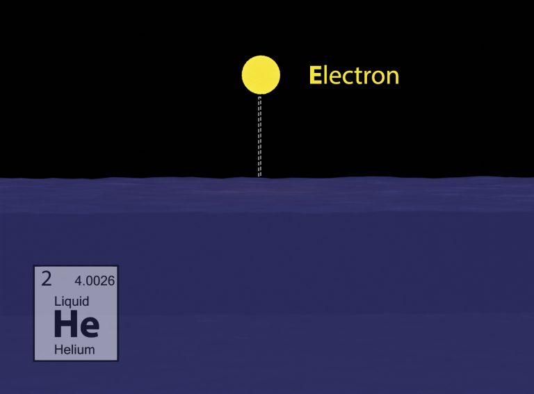
EeroQ’s approach to quantum computing is different from any other company. At the heart of any quantum processor is a qubit, and EeroQ’s qubit will be the spin of an electron floating on the surface of liquid helium.
Based on these initial ideas, and subsequent technological breakthroughs, at EeroQ we will ultimately fabricate the majority of our future processors on single chips manufactured in a commercial CMOS foundry. Once the wafers arrive from the foundry, we’ll add a thin layer of liquid helium, deposit electrons into on-chip reservoirs, initialize their spin states, and begin a computation. The electron qubit will rest about 10 nanometers above the helium surface, where it is trapped above electrodes located beneath the helium by control voltages.
EeroQ is building next-generation quantum devices by combining the tiny size of electrons and superfluid helium which is the cleanest environment in nature with CMOS infrastructure and the lack of any need for modular interconnects. These efforts, along with an efficient fabless production model, put us in a position to lead the industry.
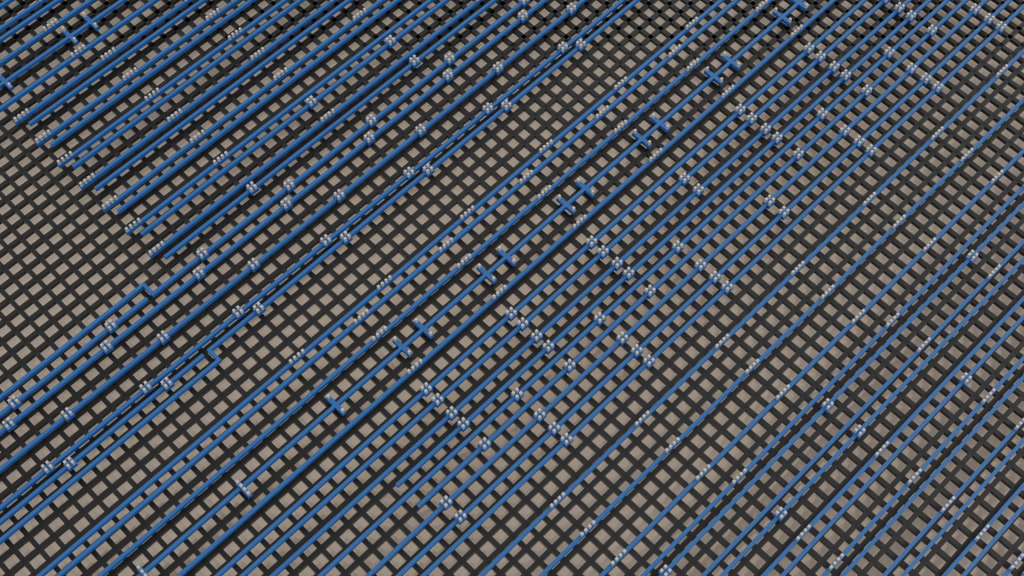
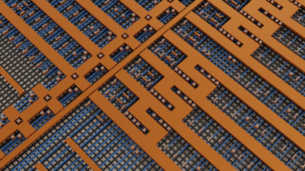
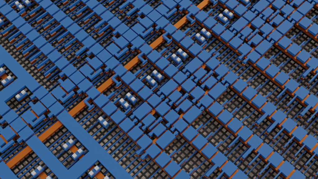
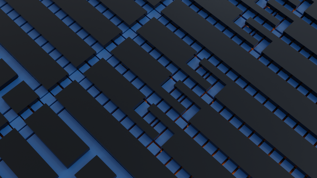
Click on the images below to scan through the layers of the chip
What’s next?
After six years of stealth work, we now have an architecture to scale this system. Since receiving fifty identical copies of our Wonder Lake chips in December 2023, we’ve been working at our Chicago headquarters, trapping and measuring electrons on them. So far, we’ve been able to isolate and measure small packets of fewer than 10 electrons on our chips, and can controllably shuttle around those packets to predetermined locations on the device. The precise spatial control of electrons that we have achieved with Wonder Lake unlocks the all-to-all connectivity needed to make future error-corrected codes and large scale quantum algorithms a reality.
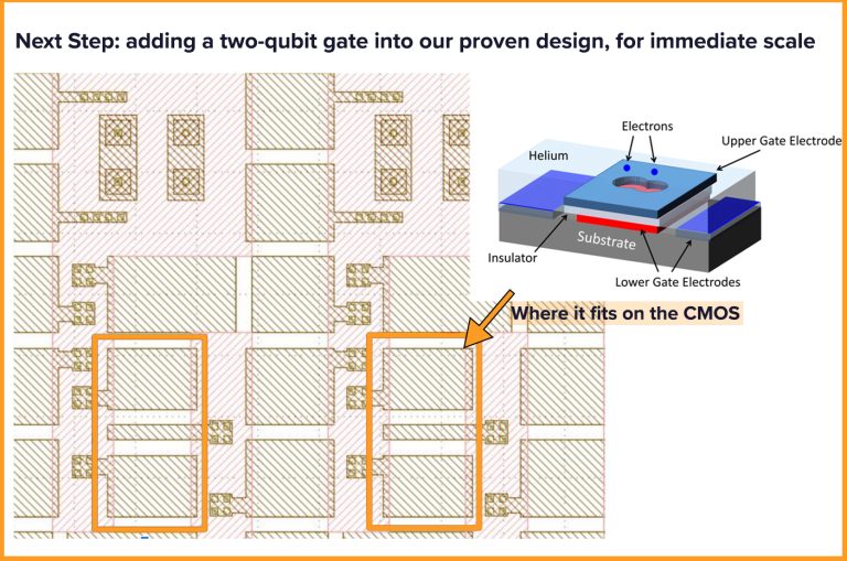
The next step is the demonstration of a two-qubit gate based on the well-understood physics of the magnetic dipole-dipole interaction, which can be “drag and dropped” onto the foundry chip.
Our first two-qubit gates will be produced by the 2 magnetic spins of the electrons. Each electron has a magnetic field, and that field is one of the most accurately known quantities in physics; the magnitude being known to at least 12 digits of precision.
In this scheme, the main source of imprecision in the entangling gate comes from the positioning of the 2 electrons, which will be controlled by engineering the microstructures on the CMOS chip that hold the electrons. The precision of the CMOS process will reduce fabrication related quantum gate errors to about 0.01%. We will then add our quantum gates to pre-designated locations on the chip, as shown below.
EeroQ’s Advantage
The work we have accomplished at EeroQ is a significant step on the road to building a commercially viable quantum computer and has allowed us to pursue our next near-term goals:.
● 10+ second qubit coherence
● High qubit connectivity
● Identical qubits, controllable in parallel with only a few voltages on a CMOS chip
● Mobile qubits on the helium surface (providing up to a 50x reduction in overhead needed for error correction)
● 99.9% gate fidelities
● A system without modular interconnects … so that all the quantum computing power you’ll need will be in a device the size of your thumbnail!
There are two particularly challenging parts to making a useful quantum computer: high-quality quantum gates, and a path to scale. With our latest work, we are proud to join the leadership ranks on scalability. Together with recent advances in error mitigation and more efficient algorithms, we can see the commercial quantum future coming together sooner than expected – led by the ability to leverage our architectural advantage to scale rapidly.